Multi-Layer Circuit Boards
Multi-Layer Circuit Boards Delivered On Time
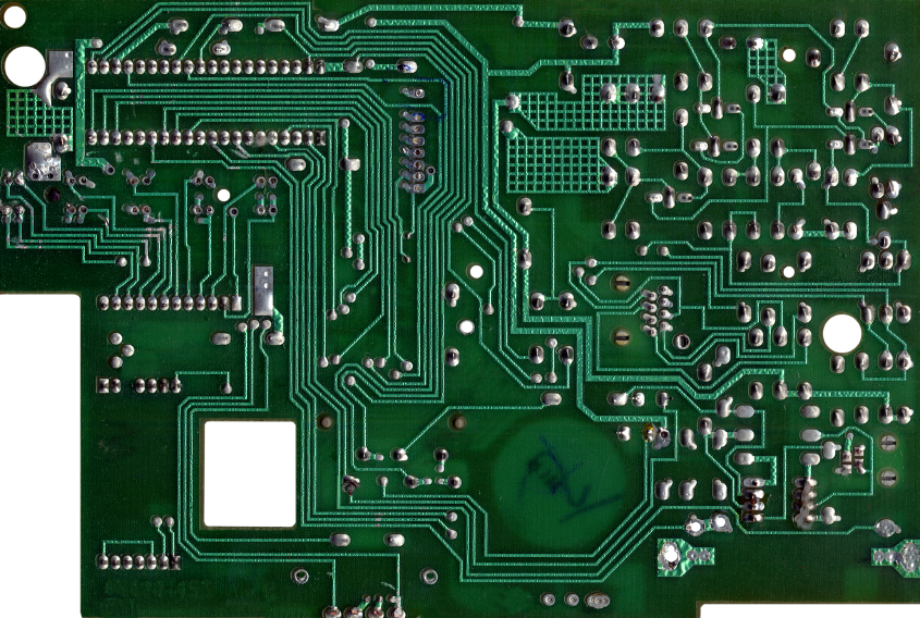
Multi‐layered printed circuit boards are a very common member of the printed circuit board family. They consist of three – twenty conductive layers and one layer of solder mask insulating layer on the top and bottom. Standard overall thicknesses range from .031” ‐ .125”. The capability to provide EMI shielding layers makes them useful for the most complex electronic applications such as mother boards and radio frequency (RF) boards. All component types can be attached to multi‐layered circuits and current carrying capabilities of signal traces range from a few milliamps to several amps.
We understand the hassle of delays and product returns, that’s why we ensure on time delivery and a 99% quality ratio across all orders for over 16 years.
Some Key Points
- Complex yet, robust construction well suited for the most complicated electronic products
- Solid rigid construction able to endure years of operation without failure
- Wide operating temperature range up to 255°C depending on the materials used
- Mount all component types – surface mount (SMT), thru – hole, wire bond, BGA
- Meets IPC‐6012 Qualifications and Performance Specifications for Rigid Printed Boards
Design Capabilities
- Layer Count: 3‐20 conductive layers
- Trace/Space: .003”/.003” typical, .002”/.002” non‐typical
- Current Carrying Capacity: few milliamps to several amps
- Hole Size: .006” drilled not plated and .008” drilled plated typical
- Copper Thickness: ½ oz, 1 oz, 2 oz typical, 3oz, 4oz non‐typical
- Material thickness: .031”, .062”, .093” and .125” typical


